
Re: Analisi foto lunari 2 - O.T.
Inviato da Iceman il 22/4/2006 14:25:08
Citazione:
Non sono informatissimo a riguardo delle novità tecnologiche che erano presenti nella missione apollo 17 rispetto alle precedenti...
credo comunque la Solita Hassemblad, ma ripeto di non essere molto informato.
Mi pare che il modulo di servizio dell apollo 17 fosse provvisto di una cinepresa le cui pellicole vennero poi recuperate con una EVA ( documentata con questa foto AS17-152-23391), non so se assieme alla cinepresa vi fosse anche una macchina fotografica(ma credo di si) e non so se l immagine della terra sia una fotografia vera e propria o il fotogramma di un filmato(ma non credo proprio, visto il codice della foto) ripreso da quella cinepresa.
Citazione:
Il postare la composizione della crosta per poi scrivere "non vi sembra un pò strano" non basta...
Non è un argomentazione!
Senza contare che per analizzare quei dati e stabilirne l attendibilità occorre almeno "masticare" qualcosa di Geologia, sennò come si può pretendere di risolvere qualcosa.
( e chissà perchè anche tra i Geologi non cè stato un "complottista")
hi-speed ha scritto:
Iceman o qualcun' altro:
con che fotocamera e pellicola hanno scattata questa foto?
as17-148-22727 (quella della terra Apollo 17)
Non sono informatissimo a riguardo delle novità tecnologiche che erano presenti nella missione apollo 17 rispetto alle precedenti...
credo comunque la Solita Hassemblad, ma ripeto di non essere molto informato.
Mi pare che il modulo di servizio dell apollo 17 fosse provvisto di una cinepresa le cui pellicole vennero poi recuperate con una EVA ( documentata con questa foto AS17-152-23391), non so se assieme alla cinepresa vi fosse anche una macchina fotografica(ma credo di si) e non so se l immagine della terra sia una fotografia vera e propria o il fotogramma di un filmato(ma non credo proprio, visto il codice della foto) ripreso da quella cinepresa.
Citazione:
qualcuno voleva dei dati scientifici e allora : Composizione della crosta (Ivan)
chi si fa avanti?
Il postare la composizione della crosta per poi scrivere "non vi sembra un pò strano" non basta...
Non è un argomentazione!
Senza contare che per analizzare quei dati e stabilirne l attendibilità occorre almeno "masticare" qualcosa di Geologia, sennò come si può pretendere di risolvere qualcosa.
( e chissà perchè anche tra i Geologi non cè stato un "complottista")
Re: Analisi foto lunari 2
Inviato da ivan il 22/4/2006 15:08:27
Vedo che siamo a corto di argomentazioni, caro Iceman.
E da un orecchio mi pare che non ci senti.
Ti ripeto la domnda nell'altro orecchio:
Perchè in quelle due foto, in una ci sono le stelle e nell'altra no?
E da un orecchio mi pare che non ci senti.
Ti ripeto la domnda nell'altro orecchio:
Perchè in quelle due foto, in una ci sono le stelle e nell'altra no?
Re: Analisi foto lunari 2
Inviato da Drive il 22/4/2006 16:48:56
Intanto il "compare" te lo tieni per te, e vedi di finirla di fare il maleducato.
Prima fai l'offeso per il "bombardare", poi quanto ti dimostro che è un termine ESATTO, per ripicca mi dai del "compare". Complimenti.
Secondo, ma tu dove le vedi le stelle e chi ti ha detto che quelle sono stelle?
Quelli sono frammenti di metallo dovuti all'apertura dell'involucro che protegge la capsula, tanto che alcune di quelle "stelle" le si vedono galleggiare anche all'interno della circonferenza del modulo.
Andiamo bene, manco le stelle riescono a distinguere questi!
Re: Analisi foto lunari 2
Inviato da Iceman il 22/4/2006 17:00:27
Citazione:
Ma dico!
Le immagini le guardi o fai finta???
In una immagine(che tra l altro mi pare essere un fotogramma di un filmato ripreso con la cinepresa!) appare al parte superiore del LM, ad essere a fuoco è un elemento scuro(il LM appunto).
I puntini dietro, come ha evidenziato Drive, non sono solo stelle ma anche e sopratutto frammenti staccati dal saturno.
Se tu visioni il filmato vedrai che alcuni dei "puntini" sembrano allontanarsi dall ultimo stadio a gran velocità... di certo non sono stelle...
Però in questa immagine si vedono anche delle stelle, perchè si tratta della riprese di un oggetto non molto illuminato.
Nell altra immagine il soggetto che viene messo a fuoco illuminato dal sole è BIANCO, per cui molto più luminoso.
Di conseguenza per metterlo a fuoco occorre ridurre molto di più l entrata di luce, cosa che "uccide" la quasi totalità della luce stellare.
Ma non ci vuole un genio...
Le stelle non si vedono se si mette a fuoco un oggetto molto illuminato.
Nella prima foto il soggetto non emana molta luce mentre nella seconda si...
ivan ha scritto:
Perchè in quelle due foto, in una ci sono le stelle e nell'altra no?
Ma dico!
Le immagini le guardi o fai finta???
In una immagine(che tra l altro mi pare essere un fotogramma di un filmato ripreso con la cinepresa!) appare al parte superiore del LM, ad essere a fuoco è un elemento scuro(il LM appunto).
I puntini dietro, come ha evidenziato Drive, non sono solo stelle ma anche e sopratutto frammenti staccati dal saturno.
Se tu visioni il filmato vedrai che alcuni dei "puntini" sembrano allontanarsi dall ultimo stadio a gran velocità... di certo non sono stelle...
Però in questa immagine si vedono anche delle stelle, perchè si tratta della riprese di un oggetto non molto illuminato.
Nell altra immagine il soggetto che viene messo a fuoco illuminato dal sole è BIANCO, per cui molto più luminoso.
Di conseguenza per metterlo a fuoco occorre ridurre molto di più l entrata di luce, cosa che "uccide" la quasi totalità della luce stellare.
Ma non ci vuole un genio...
Le stelle non si vedono se si mette a fuoco un oggetto molto illuminato.
Nella prima foto il soggetto non emana molta luce mentre nella seconda si...
Re: Analisi foto lunari 2
Inviato da ivan il 22/4/2006 17:44:46
Citazione:
http://www.clubfireworks.it/Mugnano3.jpg
Poi, a completamento:
http://aac.sunrise.it/magiche%20notti-2004.htm


Nell altra immagine il soggetto che viene messo a fuoco illuminato dal sole è BIANCO, per cui molto più luminoso.
Di conseguenza per metterlo a fuoco occorre ridurre molto di più l entrata di luce, cosa che "uccide" la quasi totalità della luce stellare.
Ma non ci vuole un genio...
Le stelle non si vedono se si mette a fuoco un oggetto molto illuminato.
Nella prima foto il soggetto non emana molta luce mentre nella seconda si...
http://www.clubfireworks.it/Mugnano3.jpg
Poi, a completamento:
http://aac.sunrise.it/magiche%20notti-2004.htm
Re: Analisi foto lunari 2 - O.T.
Inviato da ivan il 22/4/2006 17:46:40
Citazione:
Che c'è, ti da fastidio la cosa?
è per questo che rimani uno degli unicia continuare a postare imperterrito!
Che c'è, ti da fastidio la cosa?
Re: Analisi foto lunari 2
Inviato da Alb il 22/4/2006 18:46:35
Citazione:
Quelle sono foto fatte alla luce della Luna con esposizioni lunghissime. Ovvio che si vedano le stelle.
Ivan: Sarà, ma la cosa non mi convince.
Quelle sono foto fatte alla luce della Luna con esposizioni lunghissime. Ovvio che si vedano le stelle.
Re: Analisi foto lunari 2
Inviato da ivan il 22/4/2006 18:54:54
Citazione:
http://aac.sunrise.it/comete/ikeya-marzo.htm


Quelle sono foto fatte alla luce della Luna con esposizioni lunghissime. Ovvio che si vedano le stelle.
http://aac.sunrise.it/comete/ikeya-marzo.htm
Re: Analisi foto lunari 2
Inviato da Alb il 22/4/2006 18:56:25
Citazione:
?
http://aac.sunrise.it/comete/ikeya-marzo.htm
?
Re: Analisi foto lunari 2
Inviato da antony80 il 22/4/2006 19:15:32
IVAN MA IN CHE IN LINGUA TE LO DEVO DIRE CHE NON DEVI POSTARE FOTO GIGANTESCHE.
IMPIEGO 3 ORE PER CARICARE LA PAGINA LO CAPISCI O NO!!
ORA PROTESTERò PURE CON LA REDAZIONE.
IMPIEGO 3 ORE PER CARICARE LA PAGINA LO CAPISCI O NO!!
ORA PROTESTERò PURE CON LA REDAZIONE.
Re: Analisi foto lunari 2
Inviato da ivan il 22/4/2006 19:46:16
Citazione:
Che cosa strana. Il mio pc ci mette meno di un secondo a caricare tutto.
Mi sa che siete veramente a corto di argomentazioni.
IVAN MA IN CHE IN LINGUA TE LO DEVO DIRE CHE NON DEVI POSTARE FOTO GIGANTESCHE.
IMPIEGO 3 ORE PER CARICARE LA PAGINA LO CAPISCI O NO!!
ORA PROTESTERò PURE CON LA REDAZIONE.
Che cosa strana. Il mio pc ci mette meno di un secondo a caricare tutto.
Mi sa che siete veramente a corto di argomentazioni.
Re: Analisi foto lunari 2
Inviato da ivan il 22/4/2006 19:59:18
In ogni caso caro Antony:
1) Avere un hardware adeguato mi pare il requisito minimo che uno deve avere se vuole parlare su Internet di foto. Se non hai un pc all'altezza del forum, non vedo cosa c'entra il sottoscritto.
2) Le foto non erano gigantesche, il mio pc le carica in meno di un secondo e le visualizza per intero.
3) Chi se tu per dirmi (anzi, per urlarmi) quello che devo o non devo postare. Ci deve esserci una specia di epidemia ultimamente.
Re: Analisi foto lunari 2
Inviato da antony80 il 22/4/2006 19:59:23
post rimosso
maxgallo
------------------------------------
raffreddare gli animi please
maxgallo
------------------------------------
raffreddare gli animi please
Re: Analisi foto lunari 2
Inviato da ivan il 22/4/2006 20:01:49
post rimosso
maxgallo
------------------------
raffreddare gli animi please
maxgallo
------------------------
raffreddare gli animi please
Re: Analisi foto lunari 2
Inviato da ivan il 22/4/2006 20:28:38
Citazione:
http://www-xray.ast.cam.ac.uk/xray_introduction/History.html
Citazione:
http://www.astrored.org/astrofotos/apod/index.php/ap960929.html
Citazione:
http://www.airynothing.com/high_energy_tutorial/sources/moon.html
Citazione:

Citazione:
http://wwwit.kodak.com/global/it/service/publications/tib5201b.jhtml
Citazione:
Non esposta ai raggi X

Esposta ai raggi X

E alla cosa non c'è rimedio:
Citazione:
Che radiazioni INCREDIBILI ci sarebbero di così inaffrontabili??? Sopratutto considerato che le uniche radiazioni veramente pericolose per un periodo così breve sarebbero state quelle solari in presenza di un emissione maggiore(quindi in caso di tempeste particolarmente violente ecc) che però potevano essere previste ed evitate...
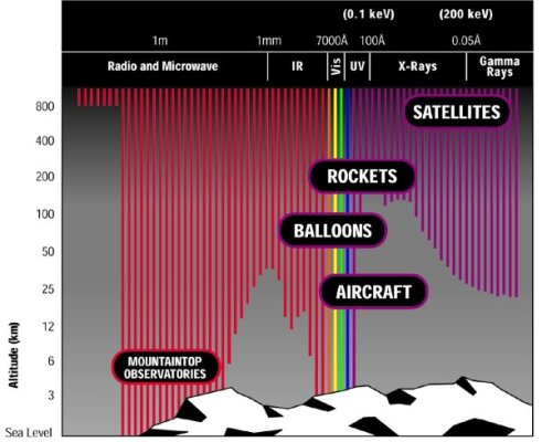
http://www-xray.ast.cam.ac.uk/xray_introduction/History.html
Citazione:
The depth of penetration of different frequencies of light into the Earths atmosphere. This shows why we need satellites for X-ray astronomy.
http://www.astrored.org/astrofotos/apod/index.php/ap960929.html
Citazione:
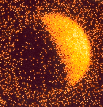
This X-Ray image of the Moon was made by the orbiting Roentgen Observatory Satellite ( ROSAT ) in 1990. It shows three distinct regions: a bright X-ray sky, a bright part of the Moon, and a relatively dark part of the Moon. The bright X-ray sky is due to the diffuse cosmic X-ray background . The bright lunar crescent shines because it reflects X-rays emitted by the Sun . The dark lunar face is in shadow and so stands stands out from the relatively bright background - but, surprisingly it is not completely dark! Where do those X-rays from? They are currently thought to result from energetic particles from the solar wind bombarding the lunar surface.
http://www.airynothing.com/high_energy_tutorial/sources/moon.html
Citazione:
The Gamma-Ray Moon
Here is an image of the Moon taken in gamma-rays:
....
The gamma rays from the Moon do not come from reflected gamma rays of the Sun. Instead, high energy particles (mostly protons) that are travelling very close to the speed of light, called cosmic-rays, continuously slam into the Moon. When these particles collide with the lunar surface, they react with the particles in the Moon's surface, exciting them and generating gamma rays
...
The Moon is brigher in gamma rays than the quiet Sun!
Citazione:
E che effetto avrebbero dovuto avere sulle pellicole???? Nel vuoto???
Non capisco proprio il problema!
Non si danneggiano i circuiti elettrici(ben più sensibili alle radiazioni!) e si dovrebbe danneggiare una pellicola???
http://wwwit.kodak.com/global/it/service/publications/tib5201b.jhtml
Citazione:
Velatura causata dai raggi X
La velatura provocata dai nuovi scanner per i bagagli è di solito più accentuata di quella causata da altri mezzi. La velatura causata dallo scanner tipo TAC di solito produce strisce larghe da 1 cm a 1,5 cm con i bordi sfumati. L'orientamento della striscia dipende dalla posizione della pellicola rispetto al fascio di raggi X. La striscia può essere ondeggiante o lineare e può essere disposta orizzontalmente o verticalmente sulla pellicola. Può essere anche ondulata, a seconda della combinazione dell'angolo di esposizione e del numero di avvolgimenti della pellicola (vedere immagini di seguito). Tuttavia, la velatura in genere non avrà i segni più tenui prodotti dalle tradizionali apparecchiature a raggi X. Inoltre, questa striscia è più o meno visibile sulle stampe a seconda del contenuto della foto. Le immagini dettagliate che ritraggono fiori, foglie, ecc. possono mascherare o ridurre gli effetti dei raggi X.
Aspetto della velatura
*
Su negativi in bianco e nero - Aree scure come descritto sopra.
*
Su negativi a colori - Aree scure con segni neutri o marroni.
*
Su pellicole di diapositive a colori - Area a densità negativa (chiazze chiare) con segni come descritto sopra.
La velatura causata dalle scansioni ad alta intensità dell'intero bagaglio danneggia tutto il negativo, quindi l'immagine appare sovresposta e a grana grossa. Le immagini scure o nere possono apparire verdi.
Altre condizioni che producono effetti simili alla velatura da raggi X
Determinate condizioni di conservazione delle pellicole possono provocare effetti molto simile alla velatura da raggi X. Più la pellicola è vecchia, più accumula radiazioni attiniche . Con il passare del tempo, le radiazioni presenti nell'ambiente velano gradualmente la grana di alogenuro d'argento più sensibile e la pellicola appare più granulosa. Questo fenomeno si nota maggiormente sulle pellicole da 800 o più sensibili. Anche conservando la pellicola in un luogo fresco o congelandola NON è possibile evitare questo problema. Con il tempo, le radiazioni penetrano o si generano in modo naturale in quasi tutti i materiali.
Il calore può alterare la scala delle tonalità e i colori della pellicola, causando degli effetti simili alla velatura da raggi X. L'entità dei danni dipende dal tipo di pellicola e dalle condizioni di conservazione.
In genere, si possono distinguere i tipi più comuni di velatura da raggi X dai tipici motivi e dalla grana più grossa. Sulle pellicole da 35 mm, le strisce in senso antiorario sono spesso confuse con la velatura da raggi X. Tuttavia, queste strisce sono più prominenti e intervallate in modo più uniforme e tendono a curvarsi in direzione opposta alle perforazioni della pellicola.
Come menzionato in precedenza, la scansione effettuata con alcuni tipi di apparecchiature di sicurezza degli aeroporti produce strisce di densità positiva (chiazze scure) o di densità negativa (chiazze chiare). La velatura può assomigliare a una tipica striscia di luce bianca , come ad esempio quella prodotta dalla luce penetrata da un piccolo foro nell'apparecchiatura. Le caratteristiche tipiche della velatura causata dall'apparecchiatura tipo TAC sono l'ampiezza ben definita delle strisce e una densità uniforme, con una grana più grossa all'interno della striscia. In genere, la striscia si estende su tutta la lunghezza del rullo o è interrotta a causa dell'avvolgimento della pellicola.
La scansione totale del bagaglio effettuata con l'apparecchiatura a raggi X produce una velatura e una grana grossa sull'intera immagine o sull'intero rullo di pellicola.
Non esposta ai raggi X
Esposta ai raggi X
E alla cosa non c'è rimedio:
Citazione:
La velatura non può essere corretta nel laboratorio fotografico
Il laboratorio fotografico non può separare la velatura causata dai raggi X dall'esposizione della fotocamera. Inoltre, siccome la velatura appare spesso a zone, è impossibile correggere questo difetto nel processo di duplicazione o di stampa. Quindi, è necessario fare il possibile per evitare che le pellicole passino attraverso i dispositivi per il controllo bagagli.
Re: Analisi foto lunari 2
Inviato da ivan il 23/4/2006 11:09:35
Citazione:
Date un'occhiata qui:
http://radhome.gsfc.nasa.gov/radhome/Nat_Space_Rad_Haz.htm
Notare:
Citazione:
Che radiazioni INCREDIBILI ci sarebbero di così inaffrontabili??? Sopratutto considerato che le uniche radiazioni veramente pericolose per un periodo così breve sarebbero state quelle solari in presenza di un emissione maggiore(quindi in caso di tempeste particolarmente violente ecc) che però potevano essere previste ed evitate...
Date un'occhiata qui:
http://radhome.gsfc.nasa.gov/radhome/Nat_Space_Rad_Haz.htm
Notare:
Citazione:
Solar Particles
The particles from solar events are a concern for spacecraft designers. In fact, for spacecraft in orbits exposed to these particles, they are often the driver for setting single event effects requirements. At this time there is no method for predicting when these events will occur.
Re: Analisi foto lunari 2
Inviato da ivan il 23/4/2006 11:31:04
Citazione:
http://ilewg.lpi.usra.edu/resources/apollo/catalog/70mm/magazine/?148
Citazione:
http://www.nasm.edu/GALLERIES/ATTM/nojs/a11.om.ap.1.html
Citazione:

Ma dico!
Le immagini le guardi o fai finta???
In una immagine(che tra l altro mi pare essere un fotogramma di un filmato ripreso con la cinepresa!)
....
Se tu visioni il filmato vedrai ...
http://ilewg.lpi.usra.edu/resources/apollo/catalog/70mm/magazine/?148
Citazione:
70mm Hasselblad Image Catalog
Apollo 17, Magazine NN
Images AS17-148-22607 to AS17-148-22775
.....
The Apollo Image Atlas is a comprehensive collection of Apollo-Saturn mission photography. Inluded are almost 25,000 lunar images, both from orbit and from the moon's surface, as well as photographs of the earth, astronauts and mission hardware.
....
70mm Hasselblad
http://www.nasm.edu/GALLERIES/ATTM/nojs/a11.om.ap.1.html
Citazione:
LUNAR SURFACE 70mm HASSELBLAD CAMERA
Used for lunar surface color still photography. This camera was adapted from the commercial Hasselblad Superwide Angle camera and could operate on Earth, in space and on the Moon without modification.
70mm HASSELBLAD CAMERA
Re: Analisi foto lunari 2
Inviato da Alb il 23/4/2006 12:15:45
Citazione:
Continuo a non capire cosa vuoi dimostrare con queste 2 foto di comete.
Ivan: -citazione-[...
Quelle sono foto fatte alla luce della Luna con esposizioni lunghissime. Ovvio che si vedano le stelle.
...]
http://aac.sunrise.it/comete/ikeya-marzo.htm
Continuo a non capire cosa vuoi dimostrare con queste 2 foto di comete.
Re: Analisi foto lunari 2
Inviato da ivan il 23/4/2006 12:19:41
Che si sarebbero potuti sprecare un pò di più.
Re: Analisi foto lunari 2 - O.T.
Inviato da ivan il 23/4/2006 12:21:42
Citazione:
http://en.wikipedia.org/wiki/Radiation_hardening
Citazione:
Non si danneggiano i circuiti elettrici(ben più sensibili alle radiazioni!) e si dovrebbe danneggiare una pellicola???
http://en.wikipedia.org/wiki/Radiation_hardening
Citazione:
Radiation effects on electronics
[edit]
Fundamental mechanisms
Two fundamental damage mechanisms take place:
* Lattice displacement, caused by neutrons, protons, alpha particles, heavy ions, and very high energy gamma photons. They change the arrangement of the atoms in the lattice, creating lasting damage, and increasing the number of recombination centers, depleting the minority carriers and worsening the analog properties of the affected semiconductor junctions. Counterintuitively, higher doses over short time cause partial annealing ("healing") of the damaged lattice, leading to lower degree of damage than with the same doses delivered in low intensity over a long time. This type of damage is especially important for bipolar transistors, which are dependent on minority carriers in their base regions; increased losses caused by recombination cause loss of the transistor gain. See neutron effects.
* Ionization effects, caused by charged particles, including the ones with energy too low to cause lattice effects. The ionization effects are usually transient, creating glitches and soft errors, but can lead to destruction of the device if they trigger other damage mechanisms, eg. a latchup. Photocurrent caused by ultraviolet and x-ray radiation may belong to this category as well. Gradual accumulation of holes in the oxide layer in MOSFET transistors leads to worsening of their performance, up to device failure when the dose is high enough; see total ionizing dose effects.
The effects can vary wildly depending on all the parameters - the type of radiation, total dose and the radiation flux, combination of types of radiation, and even the kind of the device load (operating frequency, operating voltage, actual state of the transistor during the instant it is struck by the particle), which makes thorough testing difficult, time consuming, and requiring a lot of test samples.
[edit]
Resultant effects
The "end-user" effects can be characterized in several groups:
* Neutron effects : A neutron interacting with the semiconductor lattice will displace its atoms. This leads to increase of the count of recombination centers and deep-level defects, reducing the lifetime of minority carriers, thus affecting bipolar devices more than CMOS ones. Bipolar devices on silicon tend to show changes in electrical parameters at levels of 1010 to 1011 neutrons/cm2, CMOS devices aren't affected until 1015 neutrons/cm2. The sensitivity of the devices may increase together with increasing level of integration and decreasing size of individual structures. There is also the risk of induced radioactivity caused by neutron activation, which is a major source of noise in high energy astrophysics instruments. Induced radiation, together with residual radiation from impurities in used materials, can cause all sorts of single-event problems during the device's lifetime. GaAs LEDs, common in optocouplers, are very sensitive to neutrons. Kinetic energy effects (namely lattice displacement) of charged particles belong here too.
* Total ionizing dose effects : The cumulative damage of the semiconductor lattice (lattice displacement damage) caused by ionizing radiation over the exposition time. It is measured in rads and causes slow gradual degradation of the device's performance; total dose greater than 5000 rads delivered to silicon-based devices in seconds to minutes will cause long-term degradation. In CMOS devices, the radiation creates electron-hole pairs in the gate insulation layers, which cause photocurrents during their recombination, and the holes trapped in the lattice defects in the insulator create a persistent gate bias and influence the transistors' threshold voltage, making the N-type MOSFET transistors easier and the P-type ones more difficult to switch on. The accumulated charge can be high enough to keep the transistors permanently open (or closed), leading to device failure. Some self-healing takes place over time, but this effect is not too significant.
* Transient dose effects : The short-time high-intensity pulse of radiation, typically occurring during a nuclear explosion. The high radiation flux creates photocurrents in the entire body of the semiconductor, causing transistors to randomly open, changing logical states of flip-flops and memory cells. Permanent damage may occur if the duration of the pulse is too long, or if the pulse causes junction damage or causes a latchup. Latchups are commonly caused by the x-rays and gamma radiation flash of a nuclear explosion.
* Systems-generated EMP effects (SGEMP) are caused by the radiation flash traveling through the equipment and causing local ionization and electric currents in the material of the chips, circuitboards, cables and cases.
* Single-event effects (SEE) are phenomenons affecting mostly only digital devices; see the following section for an overview of the various types of SEE.
[edit]
Digital damage: SEE
Single-event effects (SEE), mostly affecting only digital devices, were not studied extensively until relatively recently. When a high-energy particle travels through a semiconductor, it leaves an ionized track behind. This ionization may cause a highly localized effect similar to the transient dose one - a benign glitch in output, a less benign bit flip in memory or a register, or, especially in high-power transistors, a destructive latchup and burnout. Single event effects have importance for electronics in satellites, aircrafts, and other both civilian and military aerospace applications. Sometimes in circuits not involving latches it is helpful to introduce RC time constant circuits, slowing down the circuit's reaction time beyond the duration of a SEE.
* Single-event upsets (SEU), also called "soft errors" or transient radiation effects in electronics, are state changes of memory or register bits caused by a single ion interacting with the chip. They do not cause lasting damage. In very sensitive devices, a single ion can cause a multiple-bit upset (MBU) in several adjacent memory cells. SEUs can become Single-event Functional Interrupts (SEFI) when they cause placing the device into an undefined state, a test mode, or a halt, which needs a reset or a power cycle for a recovery.
* Single-event latchup (SEL) can occur in any chip with a parasitic PNPN structure. A heavy ion or a high-energy proton passing through one of the two inner-transistor junctions can open the thyristor-like structure, which then stays opened (an effect known as latchup) until the device is power-cycled. As the effect can happen between the power source and substrate, destructively high current can be involved and the part may fail. Bulk CMOS devices are most susceptible.
* Single-event transient (SET) happens when the charge collected from an ionization event discharges in the form of a spurious signal traveling through the circuit. This is de facto the effect of an electrostatic discharge.
* Single-event snapback, similar to SEL but not requiring the PNPN structure, can be induced in N-channel MOS transistors switching large currents, when an ion hits near the drain junction and causes avalanche multiplication of the charge carriers. The transistor then opens and stays opened.
* Single-event induced burnout (SEB) may occur in power MOSFETs when the substrate right under the source region gets forward-biased and the drain-source voltage is higher than the breakdown voltage of the parasitic structures. The resulting high current and local overheating then may destroy the device.
* Single-event gate rupture (SEGR) was observed in power MOSFETs when a heavy ion hits the gate region while a high voltage is applied to the gate. A local breakdown then happens in the insulating layer of silicon dioxide, causing local overheat and destruction (looking like to a microscopic explosion) of the gate region. It can occur even in EEPROM cells during write or erase, when the cells are subjected to a comparatively high voltage.
Re: Analisi foto lunari 2
Inviato da Alb il 23/4/2006 12:29:58
Citazione:
Sprecare a fare cosa ?
Non avertene a male, ma anche tu potresti sprecarti un po' di più a farti capire in quello che vuoi dire. Già stai investendo una quantità enorme di tempo a cercare riferimenti su internet (tempo che io non posso investire a cercare risposte adeguate), in proporzione cosa ti costa scrivere quello che vuoi intendere invece di costringere gli altri a chiederti innumerevoli volte cosa vuoi dire ? Per le foto delle comete siamo già alla terza mia domanda e ancora non so cosa vuoi dire, e tantomeno ho ricevuto risposta intelligibile riguardo alle foto notturne alle quali io ti ho dato risposta. Ovvio che sei libero di riempire il forum con quanta roba vuoi tu (finché il padrone di casa è disposto ad accettarlo), e di non rispondere quando non vuoi rispondere, ma più passa il tempo e più noto che te la canti e te la suoni da solo, proprio perché nessuno ha la possibilità di starti dietro. Tra poco farai un monologo che non so a chi possa giovare.
Iva: Che si sarebbero potuti sprecare un pò di più.
Sprecare a fare cosa ?
Non avertene a male, ma anche tu potresti sprecarti un po' di più a farti capire in quello che vuoi dire. Già stai investendo una quantità enorme di tempo a cercare riferimenti su internet (tempo che io non posso investire a cercare risposte adeguate), in proporzione cosa ti costa scrivere quello che vuoi intendere invece di costringere gli altri a chiederti innumerevoli volte cosa vuoi dire ? Per le foto delle comete siamo già alla terza mia domanda e ancora non so cosa vuoi dire, e tantomeno ho ricevuto risposta intelligibile riguardo alle foto notturne alle quali io ti ho dato risposta. Ovvio che sei libero di riempire il forum con quanta roba vuoi tu (finché il padrone di casa è disposto ad accettarlo), e di non rispondere quando non vuoi rispondere, ma più passa il tempo e più noto che te la canti e te la suoni da solo, proprio perché nessuno ha la possibilità di starti dietro. Tra poco farai un monologo che non so a chi possa giovare.
Re: Analisi foto lunari 2
Inviato da ivan il 23/4/2006 12:54:10
Io invece ho l'impressione che non sei in grado di controdedurre.
Le foto dimostrano l'inconsistenza di certe affermazioni.
Dimostrano pure che con mezzi molto modesti, dei modesti cultori dell'astronomia hanno ottenuto risultati fotografici migliori , ma molto migliori e sopratutto molto più consistenti di altri cultori dell'astronomia che avevavo a loro disposizione risorse economiche e materiali immense.
Ma forse questo è il punto: "quelli" non erano cultori dell'astronomia.
Re: Analisi foto lunari 2
Inviato da Alb il 23/4/2006 13:46:44
Citazione:
Ovvio che non sono in grado di controdedurre, visto che non vuoi in alcun modo chiarire cosa vuoi sapere. Ti stò chiedendo da un po' cosa c'entrano le foto delle comete e o non rispondi, o tergiversi.
Se fai una domanda precisa ed intelligibile, il sottoscritto, se sa cosa risponderti, risponde; se non sa cosa risponderti ti dice che non sa cosa risponderti. Sono enormemente ignorante e non pretendo di essere altrimenti, come ogni persona normale. Una discussione normale dovrebbe procedere su uno, massimo due fronti alla volta. Si pone una domanda, si danno risposte, si approfondisce, ed alla fine si passa oltre col prossimo argomento.
Ripeto ancora che non mi hai detto ancora nulla riguardo alle foto notturne e riguardo alle foto delle comete. Io ti ho risposto, tu no, e se l'hai fatto ti sei capito da solo e (forse volutamente) non hai dato modo a nessuno di capirti.
Ivan: Io invece ho l'impressione che non sei in grado di controdedurre.
Ovvio che non sono in grado di controdedurre, visto che non vuoi in alcun modo chiarire cosa vuoi sapere. Ti stò chiedendo da un po' cosa c'entrano le foto delle comete e o non rispondi, o tergiversi.
Se fai una domanda precisa ed intelligibile, il sottoscritto, se sa cosa risponderti, risponde; se non sa cosa risponderti ti dice che non sa cosa risponderti. Sono enormemente ignorante e non pretendo di essere altrimenti, come ogni persona normale. Una discussione normale dovrebbe procedere su uno, massimo due fronti alla volta. Si pone una domanda, si danno risposte, si approfondisce, ed alla fine si passa oltre col prossimo argomento.
Ripeto ancora che non mi hai detto ancora nulla riguardo alle foto notturne e riguardo alle foto delle comete. Io ti ho risposto, tu no, e se l'hai fatto ti sei capito da solo e (forse volutamente) non hai dato modo a nessuno di capirti.
Re: Analisi foto lunari 2
Inviato da Iceman il 23/4/2006 13:47:38
Citazione:
Allora Ivan, il discorso è chiarissimo e non capisco come tu possa porre dei quesiti del genere, comunque:
Nelle fotografie non si vedono le stelle perchè:
è impossibile che una pellicola riproduca un oggetto MOLTO ILLUMINATO in primo piano e anche le stelle nel cielo per il semplice molti che il Range di contrasto di una pellicola è troppo stretto, molto più stretto di quello dell occhio umano.
In pratica: o fotografi le stelle e ottieni uno schifoso pastone sfocato del suolo e degli oggetti o fotografi e metti a fuoco oggetti e suolo senza stelle.
La cosa è logica e indiscutibile! cè poco da fare, solo tu puoi pensare di metterla in dubbio!
Hai postato fotografie scattate sulla terra, con impostazioni di obbiettivo e di macchina ideali, in condizioni di illuminazione del terreno praticamente minime (addirittura scattate praticamente al buio!) e ti stupisci che si vedano le stelle?????
Non riesco a pensare a delle foto più inadatte a essere paragonate a quelle...
Prima di postare le foto le guardi????
ivan ha scritto:
Io invece ho l'impressione che non sei in grado di controdedurre.
Le foto dimostrano l'inconsistenza di certe affermazioni.
Dimostrano pure che con mezzi molto modesti, dei modesti cultori dell'astronomia hanno ottenuto risultati fotografici migliori , ma molto migliori e sopratutto molto più consistenti di altri cultori dell'astronomia che avevavo a loro disposizione risorse economiche e materiali immense.
Ma forse questo è il punto: "quelli" non erano cultori dell'astronomia.
Allora Ivan, il discorso è chiarissimo e non capisco come tu possa porre dei quesiti del genere, comunque:
Nelle fotografie non si vedono le stelle perchè:
è impossibile che una pellicola riproduca un oggetto MOLTO ILLUMINATO in primo piano e anche le stelle nel cielo per il semplice molti che il Range di contrasto di una pellicola è troppo stretto, molto più stretto di quello dell occhio umano.
In pratica: o fotografi le stelle e ottieni uno schifoso pastone sfocato del suolo e degli oggetti o fotografi e metti a fuoco oggetti e suolo senza stelle.
La cosa è logica e indiscutibile! cè poco da fare, solo tu puoi pensare di metterla in dubbio!
Hai postato fotografie scattate sulla terra, con impostazioni di obbiettivo e di macchina ideali, in condizioni di illuminazione del terreno praticamente minime (addirittura scattate praticamente al buio!) e ti stupisci che si vedano le stelle?????
Non riesco a pensare a delle foto più inadatte a essere paragonate a quelle...
Prima di postare le foto le guardi????
Re: Analisi foto lunari 2
Inviato da Alb il 23/4/2006 13:55:29
Iceman, avevo pensato anche io che Ivan stesse parlando di questo, ma mi sembra così banale che sono certo che lui voglia sapere altro... o no ? 
Re: Analisi foto lunari 2
Inviato da ivan il 23/4/2006 20:26:28
Citazione:
Io non voglio sapere niente da te, ci mancherebbe altro.
Vi erano delle afferamzioni che le foto le hanno smentito.
Sai controdedurre in merito ?
Ovvio che non sono in grado di controdedurre, visto che non vuoi in alcun modo chiarire cosa vuoi sapere
Io non voglio sapere niente da te, ci mancherebbe altro.
Vi erano delle afferamzioni che le foto le hanno smentito.
Sai controdedurre in merito ?
Re: Analisi foto lunari 2
Inviato da ivan il 23/4/2006 20:37:01
Iceman, io ho l'impressione che tu non sappia più che pesci prendere.
I reperti che ho portato dimostrano abbondantemente l'inconsitenza di certe affermazioni.
Torniamo agli space-travels.
Se uno è un cultore dell'astronomia certi paesaggi non se li lascia sfuggire.
Si attrezza con ogni tipo di accessorio, non va nello spazio con un solo tipo di pellicola, con un solo tipo di macchina, non portando filtri, non prendendo precauzioni per le radizioni e così via.
Un qualunque cultore di astronomia in situazioni del genere avrebbe fatto qualunque cosa per avere delle foto decenti di paesaggi unici e irripetibili.
Re: Analisi foto lunari 2
Inviato da Alb il 23/4/2006 21:28:52
Citazione:
Uhm... bello il giochino che continui a portare avanti. Io mi stò divertendo, per cui continuo a giocare.
Non vuoi sapere niente, ma mi chiedi di controdedurre. Ok, molto logico. Peccato che questa deve essere la quarta volta che ti chiedo su cosa vuoi che io controdeduca. Andremo avanti all'infinito, o almeno finché non scriverai chiaramente su cosa vuoi che io controdeduca, visto che le foto non mi sembra smentiscano nulla. Se smentiscono qualcosa, sarebbe molto interessante sapere cosa. Ce la fai a dircelo o devo chiederlo ancora altre N volte, con N che tende a chi sa quale numero reale ?
Dopo di che, se saprò rispondero. Se no, ti dirò che non so rispondere. Ed il tutto sarà durato 10 messaggi invece che 2.
Ivan:Io non voglio sapere niente da te, ci mancherebbe altro.
Vi erano delle afferamzioni che le foto le hanno smentito.
Sai controdedurre in merito ?
Uhm... bello il giochino che continui a portare avanti. Io mi stò divertendo, per cui continuo a giocare.
Non vuoi sapere niente, ma mi chiedi di controdedurre. Ok, molto logico. Peccato che questa deve essere la quarta volta che ti chiedo su cosa vuoi che io controdeduca. Andremo avanti all'infinito, o almeno finché non scriverai chiaramente su cosa vuoi che io controdeduca, visto che le foto non mi sembra smentiscano nulla. Se smentiscono qualcosa, sarebbe molto interessante sapere cosa. Ce la fai a dircelo o devo chiederlo ancora altre N volte, con N che tende a chi sa quale numero reale ?
Dopo di che, se saprò rispondero. Se no, ti dirò che non so rispondere. Ed il tutto sarà durato 10 messaggi invece che 2.
Re: Analisi foto lunari 2
Inviato da ivan il 23/4/2006 21:34:42
Vedo che continui a menar il can per l'aia, caro Alb.
Re: Analisi foto lunari 2
Inviato da Alb il 23/4/2006 21:40:38
Citazione:
Certo, come vuoi tu. Però tu sei certamente superiore e puoi fare una domanda precisa e intelligibile ad un essere inferiore, una deduzione precisa, un qualcosa insomma a cui io possa opporre una controdeduzione.
E intanto siamo a quota 5 e tu continui a non voler parlar chiaro per convincere te stesso che io non voglia rispondere, è un giochino che porti avanti da molto anche con gli altri.
Come li chiami tu ? Mezzucci!
Ivan: Vedo che continui a menar il can per l'aia, caro Alb.
Certo, come vuoi tu. Però tu sei certamente superiore e puoi fare una domanda precisa e intelligibile ad un essere inferiore, una deduzione precisa, un qualcosa insomma a cui io possa opporre una controdeduzione.
E intanto siamo a quota 5 e tu continui a non voler parlar chiaro per convincere te stesso che io non voglia rispondere, è un giochino che porti avanti da molto anche con gli altri.
Come li chiami tu ? Mezzucci!
Messaggio orinale: https://old.luogocomune.net/site/newbb/viewtopic.php?forum=13&topic_id=970